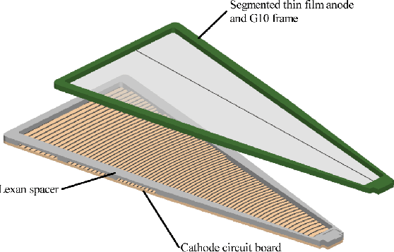
The essential elements of each PPAC comprise a thin film anode
plus a cathode circuit board. A diagram of an individual PPAC assembly is
shown in Figure 5.
 |
The anode, made of approximately 100 ![]() g/cm2 thick stretched
polypropylene with an approximately 20
g/cm2 thick stretched
polypropylene with an approximately 20 ![]() g/cm2 aluminum coating, is
glued to a 3.2 mm (0.125 in) thick G10 frame. The aluminum coating is
segmented into two electrically isolated sections to provide azimuthal angle
segmentation, one segment is
g/cm2 aluminum coating, is
glued to a 3.2 mm (0.125 in) thick G10 frame. The aluminum coating is
segmented into two electrically isolated sections to provide azimuthal angle
segmentation, one segment is
![]() wide and the other
wide and the other
![]() wide. The aluminum segments on the stretched polypropylene were made by vacuum
deposition with the back of the anode foil cooled by 0.5 torr of helium. The
vacuum deposition was performed by clamping the rear of the anode frame
against an O-ring on a similar shaped chamber that is mounted inside the
vacuum evaporator. Helium was passed through this chamber during the vacuum
deposition. The helium cooling was essential to produce coatings with good
electrical properties, anode foil coatings made not using helium cooling were
found to have dead areas.
wide. The aluminum segments on the stretched polypropylene were made by vacuum
deposition with the back of the anode foil cooled by 0.5 torr of helium. The
vacuum deposition was performed by clamping the rear of the anode frame
against an O-ring on a similar shaped chamber that is mounted inside the
vacuum evaporator. Helium was passed through this chamber during the vacuum
deposition. The helium cooling was essential to produce coatings with good
electrical properties, anode foil coatings made not using helium cooling were
found to have dead areas.
A 3.2 mm (0.125 in) thick Lexan spacer separates the anode from the
cathode. The spacer is slotted along the sides so the detector gas can
circulate to the active region of the PPAC, preventing degradation of the
detector performance over time due to radiation damage of the gas. The
azimuthal width of the spacer is 28![]() ,
and 30
,
and 30![]() for the anode
frame. The spacer has a smaller opening angle to prevent edge effects, where
the aluminized polypropylene is glued to the anode frame, from causing an
electrical discharge to the cathode. The azimuthal width of the active area of
the PPACs (defined by the spacer) is constant, so the total geometric
for the anode
frame. The spacer has a smaller opening angle to prevent edge effects, where
the aluminized polypropylene is glued to the anode frame, from causing an
electrical discharge to the cathode. The azimuthal width of the active area of
the PPACs (defined by the spacer) is constant, so the total geometric ![]() acceptance remains constant at 78% over the entire polar range of the full
detector assembly.
acceptance remains constant at 78% over the entire polar range of the full
detector assembly.
The cathode board is a three layer circuit board, shown in
Figure 6. The active side (front) of the cathode board,
where the particles are detected, is segmented into 1![]() wide traces
of constant polar angle
wide traces
of constant polar angle ![]() .
Each of the traces is connected to one
tap of a delay line which is mounted on the back side of the cathode board.
The delay line has a delay of 1 ns per tap and is made of passive delay chips
manufactured by Rhombus Industries. The traces on the active side of
the board are connected to the delay line on the back of the cathode board by
plated-thru holes which are located near the edge of the board. The third
(middle) layer is a ground plane located between the delay line side
and the active side of the cathode. The ground plane acts to capacitively
decouple the traces of the delay line on one side of the board from the
sensing traces on the active side of the board. The addition of the ground
plane considerably improves the performance of the delay line.
.
Each of the traces is connected to one
tap of a delay line which is mounted on the back side of the cathode board.
The delay line has a delay of 1 ns per tap and is made of passive delay chips
manufactured by Rhombus Industries. The traces on the active side of
the board are connected to the delay line on the back of the cathode board by
plated-thru holes which are located near the edge of the board. The third
(middle) layer is a ground plane located between the delay line side
and the active side of the cathode. The ground plane acts to capacitively
decouple the traces of the delay line on one side of the board from the
sensing traces on the active side of the board. The addition of the ground
plane considerably improves the performance of the delay line.
The signals from the anode and cathode are carried to the amplifiers by a
strip-line transmission line that has four 50 ohm impedance traces on a
central plane shielded on either side by ground planes. The PPAC end of the
transmission line is forked, allowing two of the traces to connect to the
cathode board and two of the traces to the segmented anode. The anode traces
on the transmission line also carry the bias voltage (![]() 400 V) to the PPAC
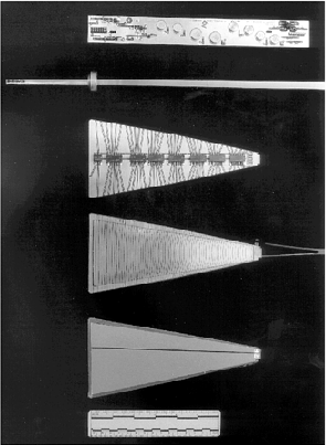
anode. Figure 7 shows a photograph of an anode, a cathode
board, transmission line and amplifier board.
400 V) to the PPAC
anode. Figure 7 shows a photograph of an anode, a cathode
board, transmission line and amplifier board.
 |